|
|
Home | Switchboard | Unix Administration | Red Hat | TCP/IP Networks | Neoliberalism | Toxic Managers |
| (slightly skeptical) Educational society promoting "Back to basics" movement against IT overcomplexity and bastardization of classic Unix | |||||||
| Computer Hardware | Recommended Links |
Samsung memory |
||||
| Motherboards | CPUs | Admin Horror Stories | Humor | Etc |
|
|
|
|
Notes:
RAM is equivalent to car engine displacement
There is no replacement for displacement
The easiest way to increase any reasonably written application performance is to increase the amount of RAM on the server. A rough idea of the performance improvement you can expect from increasing memory in your server:
Rules of thumb for adding memory
|
Memory change |
Performance gain |
|---|---|
| 1 to 2 GB | 20% to 50% |
| 2 to 4 GB | 10% to 30% |
| 4 to 8 GB | 15% to 20% |
| 8 to 16 GB | 10% to 20% |
| 16 to 32 GB | 10% to 15% |
| 32 to 64 GB | 5% to 10% |
For example, a data bus eight-bytes wide (64 bits) by definition transfers eight bytes in each transfer operation; at a transfer rate of 1 GT/s, the data rate would be 8 × 109 bytes/s, i.e. 8 GB/s, or approximately 7.45 GiB/s. The bit rate for this example is 64 Gbit/s (8 × 8 × 109 bits/s).
| DDR4-3200 | PC4-25600 | 400 MHz | 1600 MHz | 3200 MT/s | 1.2 V |
Memory in servers is implemented in the form of Dual Inline Memory Modules (DIMMs).
See DIMM - Wikipedia, the free encyclopedia
DIMMs contain a number of chips, known as Synchronous Dynamic RAM (SDRAM or just DRAM) chips. The number of chips implemented on the DIMM depends on the total capacity of the DIMM and whether the DIMM has error checking and correcting (ECC) functions. Without ECC, a DIMM typically has 8 or 16 SDRAM chips. With ECC, there are typically 9 or 18 chips.
The capacity of each DRAM is a number of "words" where each word can be 4 bits ("x4"), 8 bits ("x8") and, starting to become prevalent, 16 bits in length ("x16"). The word length is usually written as x4 for 4 bits, and so on. The number of words in the DRAM is sometimes written on the label of the DIMM, such as 128M, meaning that each DRAM has 128 million (actually 128 x 10243) words.
Note: The word length (x4 or x8) is normally not printed on the label, however the DIMM manufacturer's
Web site might list such specifications. It can also be calculated:
(DIMM capacity in MB) / (Number of non-ECC DRAMs) * 8 / (M value) So for the 1 GB DIMM in 1024 MB / 8 * 8 / 128 = 8 bit word length. |
The sum of the capacities of the DRAM chips (minus any used for ECC functions if any), equals the capacity of the DIMM. Using the previous example, the DRAMs in Figure 8-2 are 8-bits wide, so:
For various technologies, there are certain bus and device clock frequencies that are standardized; there is also a decided nomenclature for each of these speeds for each type.
DIMMs based on Single Data Rate (SDR) DRAM have the same bus frequency for data, address and control lines. DIMMs based on Double Data Rate (DDR) DRAM have data but not the strobe at double the rate of the clock; this is achieved by clocking on both the rising and falling edge of the data strobes. Power consumption and voltage gradually became lower with each generation of DDR-based DIMMs.
| Chip | Module | Effective Clock | Voltage |
|---|---|---|---|
| SDR-66 | PC-66 | 66 MHz | 3.3 V |
| SDR-100 | PC-100 | 100 MHz | 3.3 V |
| SDR-133 | PC-133 | 133 MHz | 3.3 V |
| Chip | Module | Memory Clock | I/O Bus Clock | Transfer rate | Voltage |
|---|---|---|---|---|---|
| DDR-200 | PC-1600 | 100 MHz | 100 MHz | 200 MT/s | 2.5 V |
| DDR-266 | PC-2100 | 133 MHz | 133 MHz | 266 MT/s | 2.5 V |
| DDR-333 | PC-2700 | 166 MHz | 166 MHz | 333 MT/s | 2.5 V |
| DDR-400 | PC-3200 | 200 MHz | 200 MHz | 400 MT/s | 2.5 V |
| Chip | Module | Memory Clock | I/O Bus Clock | Transfer rate | Voltage |
|---|---|---|---|---|---|
| DDR2-400 | PC2-3200 | 100 MHz | 200 MHz | 400 MT/s | 1.8 V |
| DDR2-533 | PC2-4200 | 133 MHz | 266 MHz | 533 MT/s | 1.8 V |
| DDR2-667 | PC2-5300 | 166 MHz | 333 MHz | 667 MT/s | 1.8 V |
| DDR2-800 | PC2-6400 | 200 MHz | 400 MHz | 800 MT/s | 1.8 V |
| DDR2-1066 | PC2-8500 | 266 MHz | 533 MHz | 1066 MT/s | 1.8 V |
| Chip | Module | Memory Clock | I/O Bus Clock | Transfer rate | Voltage |
|---|---|---|---|---|---|
| DDR3-800 | PC3-6400 | 100 MHz | 400 MHz | 800 MT/s | 1.5 V |
| DDR3-1066 | PC3-8500 | 133 MHz | 533 MHz | 1066 MT/s | 1.5 V |
| DDR3-1333 | PC3-10600 | 166 MHz | 667 MHz | 1333 MT/s | 1.5 V |
| DDR3-1600 | PC3-12800 | 200 MHz | 800 MHz | 1600 MT/s | 1.5 V |
| DDR3-1866 | PC3-14900 | 233 MHz | 933 MHz | 1866 MT/s | 1.5 V |
| DDR3-2133 | PC3-17000 | 266 MHz | 1066 MHz | 2133 MT/s | 1.5 V |
| DDR3-2400 | PC3-19200 | 300 MHz | 1200 MHz | 2400 MT/s | 1.5 V |
| Chip | Module | Memory Clock | I/O Bus Clock | Transfer rate | Voltage |
|---|---|---|---|---|---|
| DDR4-1600 | PC4-12800 | 200 MHz | 800 MHz | 1600 MT/s | 1.2 V |
| DDR4-1866 | PC4-14900 | 233 MHz | 933 MHz | 1866 MT/s | 1.2 V |
| DDR4-2133 | PC4-17000 | 266 MHz | 1066 MHz | 2133 MT/s | 1.2 V |
| DDR4-2400 | PC4-19200 | 300 MHz | 1200 MHz | 2400 MT/s | 1.2 V |
| DDR4-2666 | PC4-21300 | 333 MHz | 1333 MHz | 2666 MT/s | 1.2 V |
| DDR4-3200 | PC4-25600 | 400 MHz | 1600 MHz | 3200 MT/s | 1.2 V |
| Note:
Transfer
(computing) - Wikipedia, the free encyclopedia In computer technology, transfers per second and its more common derivatives gigatransfers per second (abbreviated GT/s) and megatransfers per second (MT/s) are informal language that refer to the number of operations transferring data that occur in each second in some given data-transfer channel. For example, a data bus eight-bytes wide (64 bits) by definition transfers eight bytes in each transfer operation; at a transfer rate of 1 GT/s, the data rate would be 8 × 109 bytes/s, i.e. 8 GB/s, or approximately 7.45 GiB/s. The bit rate for this example is 64 Gbit/s (8 × 8 × 109 bits/s). |
Single-rank DIMMs and the double-ranked DIMMs are identified as follows in manufacturer's technical sheets, depending on the model:
| x8SR = x8 single-ranked modules - have five DRAMs on the front and four DRAMs on the back with empty spots in between the DRAMs. |
| x8DR = x8 double-ranked modules - have nine DRAMs on each side for a total of 18 (no empty slots) |
| x4SR = x4 single-ranked modules - have nine DRAMs on each side for a total of 18 and look similar to x8 double-ranked |
| x4DR = x4 double-ranked modules - have 18 DRAMs on each side for a total of 36. |
The rank of a DIMM also impacts how many failures a DIMM can tolerate using redundant bit steering. See Memory ProteXion: Redundant bit steering for details.
Synchronous Dynamic Random Access Memory (SDRAM) is the most common type of memory today, and this memory type continues to evolve to keep pace with modern processors. SDRAM enables fast, continuous bursting of sequential memory addresses. After the first address is supplied, the SDRAM itself increments an address pointer and readies the next memory location that is accessed. The SDRAM continues bursting until the predetermined length of data has been accessed. The SDRAM supplies and uses a synchronous clock to clock out data from the SDRAM chips. The address generator logic of the SDRAM module also uses the system-supplied clock to increment the address counter to point to the next address.
There are two types of SDRAMs currently on the market: registered and unbuffered. Only registered SDRAM are now used in System x servers, however. Registered and unbuffered cannot be mixed together in a server.
With unbuffered DIMMs, the memory controller communicates directly with the DRAMs, giving them a slight performance advantage over registered DIMMs. The disadvantage of unbuffered DIMMs is that they have a limited drive capability, which means that the number of DIMMs that can be connected together on the same bus remains small, due to electrical loading. Unbuffered DIMMs can manage one operation at a time.
In contrast, registered DIMMs use registers to isolate the memory controller from the DRAMs, which leads to a lighter electrical load. Therefore, more DIMMs can be interconnected and larger memory capacity is possible.
The register does, however, typically impose a clock or more of delay, meaning that registered DIMMs often have longer access times than their unbuffered counterparts. The registered DIMMs are able to mange operations in parallel.
These differences mean that fewer unbuffered DIMMs are typically supported in a system than for a design using registered DIMMs. While this might not be a problem for desktop systems, servers now need large amounts of memory and use registered DIMMs.
Data transfers made to and from an SDRAM DIMM use a synchronous clock signal to establish timing. For example, SDRAM memory transfers data whenever the clock signal makes a transition from a logic low level to a logic high level. Faster clock speeds mean faster data transfer from the DIMM into the memory controller (and finally to the processor) or PCI adapters. However, electromagnetic effects induce noise which limits how fast signals can be cycled across the memory bus.
Double Data Rate (DDR) memory techniques increase the data rate by transferring data on both the rising edge and the falling edge of the clock signal. DDR DIMMs use a 2x prefetch scheme so that two sets of 64-bit data are referenced simultaneously. Logic on the DIMM multiplexes the two 64-bit results (plus ECC bits) to appear on each of the rising and falling edges of the clock signal. Thus, two data transfers can be performed during one clock period.
DDR2 is the new generation of DDR technology.
DDR2 consumes less power than DDR and offers a higher range of throughputs because it has half the speed of the memory core (thereby reducing power consumption) but offsets that by doubling the number of prefetches from the memory core to the I/O buffers (from 2 to 4), as shown in Figure 8-4.
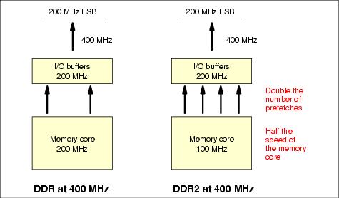
Figure 8-4 Comparing DDR and DDR2 at the same external frequency
The lower frequency at the memory core means less power consumption and the ability to increase data density (and therefore capacity) and increase speeds as manufacturing technology improves.
Note: DDR2 has 240 pins.DDR and DDR2 at the same external frequency (400 MHz dual-edge), the throughput is the same. But because the internal core frequency of DDR2 is half that of DDR, there is more scope to increase frequencies and, therefore, increase the bandwidth of DDR2. However, the lower memory core frequency means longer latency time (that is, the time it takes to set up the request for data transfer).
The end result of this is that at the DDR2 lower frequency of 400 MHz, which is the DDR upper frequency, the two technologies offer equal throughput, but the latency of DDR2 is worse. However, because DDR2 frequencies can increase (667 MHz, 800 MHz is available) and DDR has reached its limit, throughput has increased and latencies have equalized.
As CPU speeds increase, memory access must keep up so as to reduce the potential for bottlenecks in the memory subsystem. With the DDR2 parallel memory bus design, all DIMMs on the one channel are connected to the memory controller. The problem is that as the speed of the memory channel increases, the number of DIMMs that can be connected decreases due to electrical loading. One solution is to add more channels, but that requires a significantly more complex circuit board design and larger board surface area for the additional wires.
The fully-buffered DIMM (FB-DIMM) technology replaces the shared parallel memory channel that is used in traditional DDR and DDR2 memory controllers and uses a serial connection to each DIMM on the channel. As shown in Figure 8-5, the first DIMM in the channel is connected to the memory controller. Subsequent DIMMs on the channel connect to the one before it. The interface at each DIMM is a buffer known as the Advanced Memory Buffer (AMB).
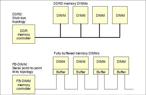
Figure 8-5 Comparing the DDR stub-bus topology with FB-DIMM serial topology
This serial interface results in fewer connections to the DIMMs (approximately 69 per channel) and less complex wiring. These links are relatively similar to the ones used for PCI-E, SATA, or SAS technologies. The interface between the buffer and DRAM chips is the same as with DDR2 DIMMs. The DRAM chips are also the same as DDR2 DIMMs.
With this serial point-to-point connectivity, this is a built-in latency associated with any memory request. In addition, the design of FB-DIMM is such that even if the request is fulfilled by the first DIMM nearest to the memory controller, the address request must still travel the full length of the serial bus. As a consequence, the more DIMMs per channel that you have, the longer the latency
Figure 8-6 shows the architecture of an FB-DIMM implementation, showing connections and placement of the buffer and DRAM chips.
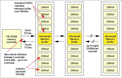
Figure 8-6 Fully buffered DIMMs architecture
Note: FB-DIMMs are not the next generation of DRAM. It is a new way of accessing the same DDR2 DRAMs from a new memory controller.
With the FB-DIMMs, the density can then increase without generating errors on data access to allow much more capacity scaling and a much larger memory bandwidth. An FB-DIMM memory controller can support up to 6 channels with up to 8 DIMMs per channel and single or dual-rank DIMMs. In addition, power consumption for an FB-DIMM is now 1.2 V versus 1.8 V for DDR2 DIMMs. Figure 8-7 shows an FB-DIMM.
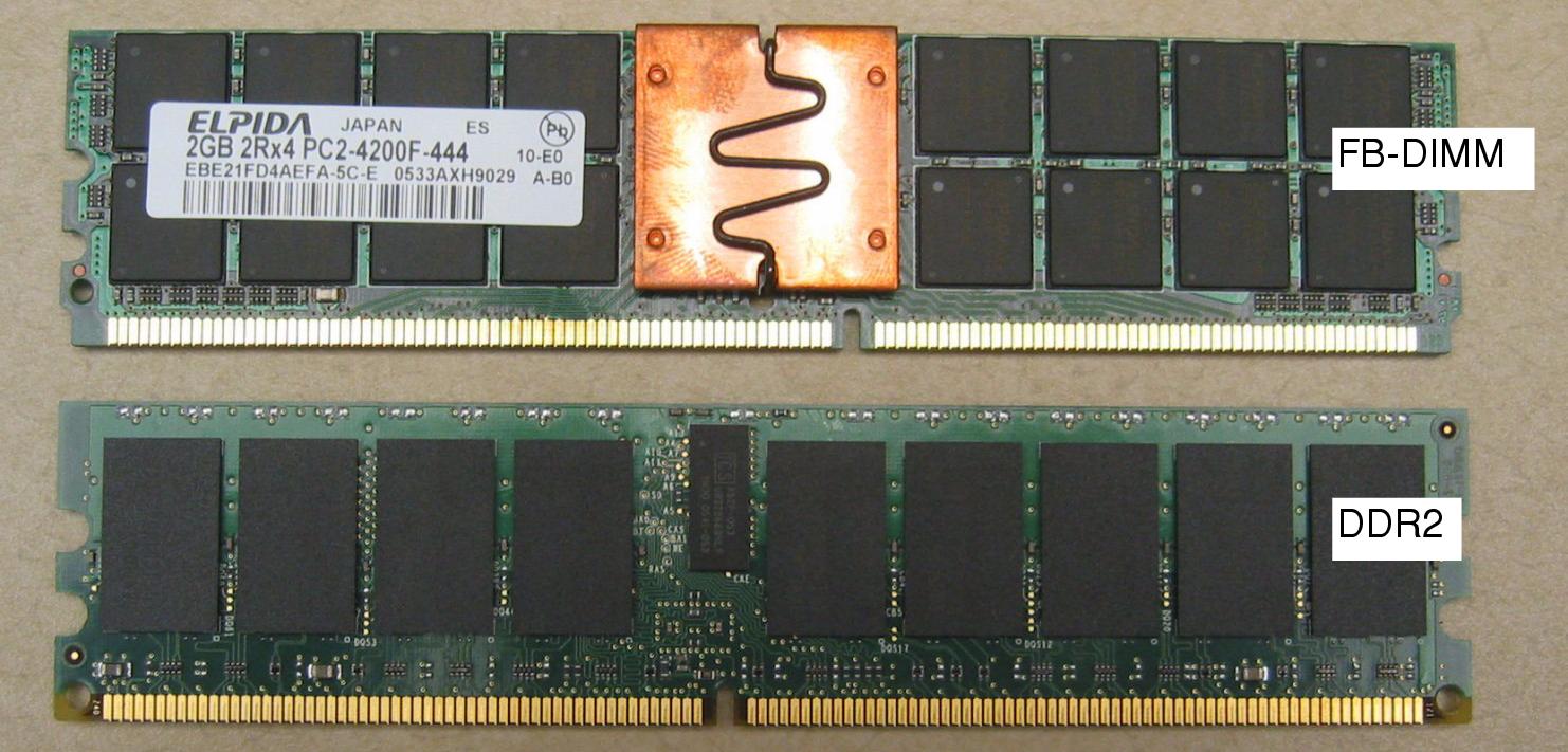
Figure 8-7 An FB-DIMM has the same connector as a DDR2 DIMM but a different key
Basically, FB-DIMMs allow for greater memory capacity in a server.
An FB-DIMM uses a buffer known as the Advanced Memory Buffer (AMB), as shown in Figure 8-8. The AMB is a memory interface that connects an array of DRAM chips to the memory controller. The AMB is responsible for handling FB-DIMM channel and memory requests to and from the local FB-DIMM and for forwarding requests to other AMBs in other FB-DIMMs on the channel.
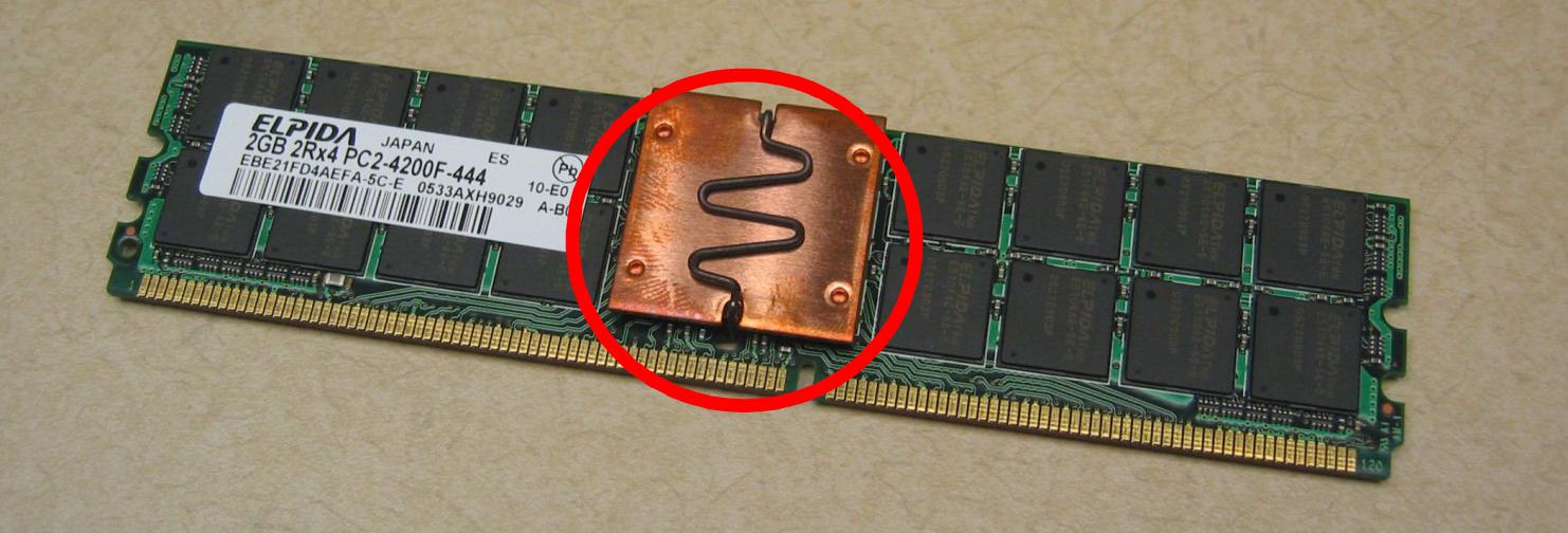
Figure 8-8 The Advanced Memory Buffer on an FB-DIMM
The functions that the AMB performs includes the following:
With a less complicated circuit board design and lower power consumption, server designers can now create memory controllers with more channels. The use of more memory channels results in better throughput.
The use of a serial connection adds latency to memory access, but the greater throughput offered by FB-DIMM results in lower average latency when under load, thereby improving performance, as shown in Figure 8-9.
Figure 8-9 shows us that with more channels, you can reach higher throughput. At low throughput levels, the latency of the serial link is significant, however because that latency remains constant regardless of the load, FB-DIMM performance is significantly better than DDR2 as throughput increases.
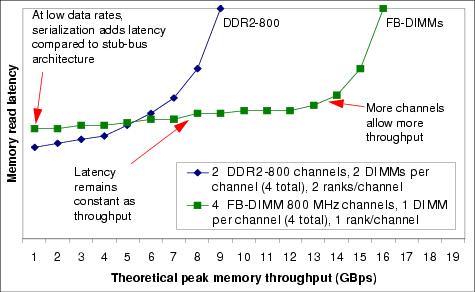
Figure 8-9 Latency versus throughput for DDR2 and FB-DIMMs
The speed of a memory DIMM is indicated by PC value, both for DDR and DDR2 DIMMs. The tables in this section list the nomenclature and the bus speed, transfer speed, and peak throughput.
With DDR and DDR2, because the SDRAM transfers data on both the falling and the rising edges of the clock signal, transfers speeds are double the memory bus speed.
DDR memory implementations
| DDR2 type | Bus speed | DDR transfers | Peak throughput |
|---|---|---|---|
| PC2-3200 | 200 MHz | 400 MHz | 3.2 GBps |
| PC2-4300 | 266 MHz | 533 MHz | 4.3 GBps |
| PC2-5300 | 333 MHz | 667 MHz | 5.3 GBps |
| PC2-6400 | 200 MHz | 800 MHz | 6.4 GBps |
DDR2 memory implementations
Because FB-DIMMs use DDR2 SDRAM, no specific name or performance changes have been introduced.
You can find more detailed SDRAM specification information at:
http://developer.intel.com/technology/memory/
In general, the DIMM location within the system's DIMM sockets does not affect server performance, although a particular server might require specific DIMM layouts for other reasons (such as initial detection of installed memory). In general, optimal performance is obtained when populating all DIMM slots with equivalent memory size DIMMs. This rule is also the case with modern DIMM technology such as DDR2 and FB-DIMM.
Using the maximum number of the same-capacity DIMMs allows the memory controller to maintain the maximum number of open memory pages. Doing so reduces memory latency and gives the memory controller the option to enable address bit permuting (sometimes called symmetric mode or enhanced memory mapping), which reorders memory addresses to reduce random and sequential memory read/write latencies significantly.
The significance of this discussion is that memory performance is highly dependent upon not just whether the data is in cache or main memory, but also how the access patterns appear to the memory controller. The access pattern will strongly affect how the memory controller reorders or combines memory requests, whether successive requests hit the same page, and so forth. Memory performance is affected by a number of complex factors. Those factors can include the choice of architecture, processor frequency, memory frequency, the number of DIMMs in the system, and whether the system is set up as a NUMA or an SMP system.
Interleaving is a technique that is often used to organize DIMMs on the motherboard of a server in order to improve memory transfer performance.
The technique can be implemented within a single cache line access or across multiple cache lines to improve total memory bandwidth. When two DIMMs are grouped together and accessed concurrently to respond to a single cache line request, the interleave is defined as two-way; when four DIMMs are grouped together and accessed concurrently for a single cache line, the interleave is four-way.
Interleaving improves memory performance because each DIMM in the interleave is given its memory address at the same time. Each DIMM begins the access while the memory controller waits for the first access latency time to expire. Then, after the first access latency has expired, all DIMMs in the interleave are ready to transfer multiple 64-bit objects in parallel, without delay (the front side bus is still 64 bits wide on the Xeon MP). Interleaving requires a 128-bit memory bus for two-way interleaving and a 256-bit memory bus for four-way interleaving.
Systems designed around the Pentium 4 processor microarchitecture (Pentium 4, Xeon DP, and Xeon MP) usually employ a minimum of two-way interleaving using DDR DIMMs. In these systems, two-way interleaving is usually configured using two banks of DDR memory DIMMs. You can also set up four-way interleaving with four banks of DDR DIMMs. In either case, the memory subsystem is capable of transferring 64 bits of data at the full front-side bus speed of 400 MHz.
The important points to remember are:
| Interleaving improves performance. If interleaving is optional, then we recommend you implement it to maximize your server investment by installing the appropriate number of DIMMs per the server documentation. |
| DDR and DDR2 have similar interleaving characteristics. |
| A single DDR or DDR2 DIMM transfers 64 bits at 200 MHz and therefore two-way DDR interleaving is required to match the 400 MHz transfer rate of the front-side bus. |
Performance with memory can be simplified into two main aspects:
Basically, the more memory bandwidth you have, the better system performance will be, because data can be transferred faster. Bandwidth can be compared as a highway: the more lines you have, the more traffic you can handle. The memory DIMMs are connected to the memory controller through memory channels, and the memory bandwidth for a system is calculated by multiplying the number of bytes of a channel from a memory controller by the number of channels, and then multiplied by the frequency of the memory (or front side bus).
For example, if a processor is able to support up to 400 MHz (DDR-400) registered ECC memory and has two 8-byte channels from the memory controller to access the memory, then the memory bandwidth of the system will be 8 bytes*2*400 MHz, or 6.4 GBps. If the memory used is DDR-333, the memory bandwidth will be 5.3 GBps.
Models that use 533 and 667 MHz memory have a theoretical bandwidth of 4.3 GBps and 5.3 GBps per channel.
| Tip: The theoretical memory bandwidth does not depend on the memory technology (DDR-1 or DDR-2), but on the memory frequency, on the number of channels and on the size of these channels. |
If the request cannot be satisfied in cache, it is forwarded on through various mechanisms to the memory controller (for example, north bridge for Xeon or MCT for Opteron). The memory controller can hold incoming read or write requests in a queue while it completes other requests that are in progress. As new requests come in, they are checked against existing requests in the queue. If the new requests are related to requests currently in the queue, they can be combined or reordered to save time.
Processors are designed to access memory using a structure called a cache line. Currently, a cache line is 64-byte wide, organized as 8 units of 64 bits (8 bytes).
The performance of memory access is usually described by listing the number of front-side bus clock cycles that are necessary for each of the 64-bit transfers needed to fill a cache line.
Cache lines are multiplexed to increase performance, and the addresses are divided into row addresses and column addresses.
A row address is the upper half of the address (that is, the upper 32 bits of a 64-bit address), while a column address is the lower half of the address. The row address must be set first, then the column address. When the memory controller is ready to issue a read or write request, the address lines are set, and the command is issued to the DIMMs.
When two requests have different column addresses but use the same row address, they are said to occur in the same page. When multiple requests to the same page occur together, the memory controller can set the column address once, and then change the row address as needed for each reference. The page can be left open until the it's no longer needed. Or it can be closed after the request is issued. We talk about respectively page open or page closed policy.
The act of changing a column address is referred to as Column Address Select or CAS.
There are actually four common access times:
 |
|
CAS: Column Address Select |
|
|
RAS to CAS: delay between row access and column access |
|
|
RAS: Row Address Strobe |
Sometimes, these numbers are expressed as x-y-y by manufacturers.
These numbers are expressed in clocks and might be interpreted as wait times or latency. Therefore, the less these numbers are the better, because access times imply data access latency. CAS Latency (CL) measures the number of memory clocks that elapse between the time a memory controller sets the column address to request a line of data and when the DIMM is able to respond with that data. Even if other latencies are specified by memory manufacturers, CL is the most commonly used when talking about latency. If you look at the sticker on a DIMM (Figure 8-10), it might list the CL value for that particular device.
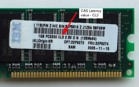
Figure 8-10 CAS Latency value as printed on a PC3200 (400 MHz) DDR DIMM
CL values:
Numbers with fractions are possible because data can be clocked at a different rate than commands.
With DDR memory, data is clocked at double the speed of commands. For example, 400 MHz DDR memory has a data clock of 400 MHz and a native clock (command and address) of 200 MHz. Thus, CL2.5 memory has a CL of 2.5 command clocks, which is equivalent to five data clocks.
When talking about latency, manufacturers generally refer to CL, which is a theoretical latency and which corresponds to an unloaded latency. A single thread that is executed by a single processor to memory (when data is not in the cache) generates memory access and therefore latency. Because one processor is accessing memory at one time, we talk about unloaded latency.
As soon as a second processor, or a second thread, concurrently accesses memory, the latency is increased and is defined as loaded latency. In NUMA architecture, if a processor accesses memory locally and another processor accesses the same memory (remotely), there are concurrent memory accesses and, therefore, loaded latency.
STREAM is a synthetic benchmark program that measures memory bandwidth in MBps and the computational rate for simple vector kernels. The benchmark is designed to work with larger data sets than the available cache on any given system so that the results are indicative of very large vector style applications. It provides real-world sustained memory bandwidth and not the theoretical peak bandwidth that is provided by vendors. You can find more information about the STREAM benchmark at:
http://www.cs.virginia.edu/stream
While STREAM gives the memory bandwidth of a given system, a good focus on latency should be made at the same time.
Because different processor manufacturers use a different architecture, memory access to and from processors differs from one solution to another. In the System x world, there are two architectures: SMP and NUMA. We discuss both of these in this section.
Both architectures have benefits and limitations, depending on the workload. System x servers with four or fewer Intel processors use the SMP architecture, while System x servers with Opteron processors exclusively use a NUMA architecture.
Systems that are based on the Intel Xeon processor typically use the Symmetric Multiprocessing (SMP) Architecture. SMP systems have a shared front-side bus that connects the processors to a single controller called a north bridge. Each processor communicates with the front-side bus through its bus interface unit (BIU).
The CPU accesses memory DIMMs through the separate memory controller or north bridge. The north bridge handles traffic between the processor and memory, controls traffic between the processor and I/O devices, and data traffic between I/O devices and memory. Figure 8-11 shows the central position of the north bridge and the shared front-side bus. These components play the dominant role in determining memory performance. A single processor is capable of saturating the front-side bus, so the second processor could compete for memory bandwidth. The processors also share memory bandwidth with I/O devices, including inter-communication devices.
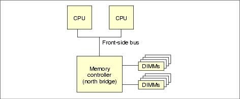
Figure 8-11 An Intel dual-processor memory block
The clock is the internal computer's components heartbeat. It is the element that defines time. A clock cycle is an upgoing and downgoing electrical signal (alternating high and low voltage). The clock frequency is the number of pulses that are emitted by a clock in one second and is measured in hertz (Hz). Memory accesses are based on clock cycles. Data is sent on rising and falling edges of clock cycles for the DDR and DDR2 (that is what double refers to, in DDR). The processor frequency, the memory bus frequency and the front-side bus frequency are different, however the memory frequency must match the memory bus frequency. The memory frequency can currently go from 200 MHz to 800 MHz. However, it is common to have the front-side bus speed and the memory bus speed matching.
The north bridge clock is tied to the speed of the front-side bus, so even as processor clock rates increase, the latency to memory remains virtually the same. The speed of the front-side bus places an upper bound on the rate at which a processor can send data to or receive data from memory. In fact, front-side bus bandwidth is often tuned to match the bandwidth of available memory technology at the time.
It is expected that a single processor will not saturate the front-side bus over time because the processor has a cache where data most likely to be referenced are stored. Cache reduces the front-side bus pressure, so there is capacity to allow more than one processor to operate on the front-side bus. For example, a two-processor Xeon system can have a front-side bus that is 8 bytes wide and clocked at 800 MHz. Its memory controller has two channels, each 8 bytes wide, to DDR-II 400 memory. This gives the front-side bus and the memory bus 6.4 GBps of bandwidth each (8B * 2 * 400 MHz).
Note: The memory frequency drives the memory controller speed (the controller cannot run faster than the memory). As well, the front-side bus limits the processor speed for accessing the memory controller. So, even if the processor speed is increased, the latency and the throughput will be the same, because it is limited by the memory speed.
Opteron has a different type of architecture-NUMA rather than SMP. The memory controller is integrated into the processor, which can be an advantage for two reasons. First, the memory controller is clocked at the same rate as the processor. So, as the processor speed is increased, the memory controller speed is also increased, which reduces the latency through the memory controller and allows faster access to memory. Second, when a processor is added to a system, more paths to memory are also added. As the demand for memory bandwidth increases due to the additional processor, more bandwidth is available to satisfy that demand.
However, with NUMA architecture and with multiple processors, a new concept is raised, remote memory. From a processor point of view, local memory refers to the memory DIMMs that are connected to the processor's integrated memory controller. Remote memory, as a consequence, refers to memory that is connected to another processors' integrated memory controller.
| Note: NUMA architecture is not specific to AMD processors. |
Figure 8-12 shows the architecture of the Opteron processor. As in Figure 8-11, there is a processor core and cache. However, in place of a bus interface unit and an external memory controller, there is an integrated memory controller (MCT), an interface to the processor core (SRQ), three coherent HyperTransportTM (cHT) units and a cross bar switch to handle routing of data, commands, and addresses between them.
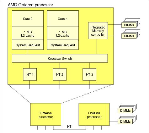
Figure 8-12 An AMD dual-processor memory block
Two of the HyperTransport (HT or cHT) units are typically used for connecting to other processors. The third HT unit is to connect to I/O devices. The protocol that is used for routing memory traffic is somewhat more elaborate than what is used for I/O. However, the I/O protocol is a subset, so cHT links can be used for either purpose.
Note that every device within the processor package is clocked using a single clock. As the processor clock is increased from one generation or processor speed bin to the next, the memory controller clock is increased automatically at the same rate. This increase has the advantage of decreasing the latency of a memory request from the processor core to the memory, which improves access. The disadvantage is that the cHT can be limiting as soon as remote memory access is made.
A memory address is a unique identifier for a memory location at which a processor or other device can store a piece of data for later retrieval. Each address identifies a single byte of storage. All applications use virtual addresses, not physical. The operating system maps any (virtual) memory requests from applications into physical locations in RAM. When the total amount of virtual memory used by all applications combined exceed the physical RAM installed, the difference is stored in the page file also managed by the operating system.
32-bit CPUs, such as the Intel Xeon, have an architectural limit of only being able to directly address 4 GB of memory. With many enterprise server applications requiring more and more memory, Intel and operating system vendors have developed methods to give applications access to more memory.
The first method was implemented by Microsoft with its Windows NT 4.0 Enterprise Edition operating system. Prior to Enterprise Edition, the 4 GB memory space in Windows was divided into 2 GB for the operating system kernel and 2 GB for applications. Enterprise Edition offers the option to allocate 3 GB to applications and 1 GB to the operating system using the 3 GB parameter in the BOOT.INI file. This modification provided a performance improvement of about 20% as measured by the TPC-C benchmark. For more information, see 11.13, The /3GB BOOT.INI parameter (32-bit x86).
The Linux kernel, by default, splits the 4 GB virtual address space of a process in two parts: 3 GB for the user-space virtual addresses and the upper 1 GB for the kernel virtual addresses. The kernel virtual area maps to the first 1 GB of physical RAM and the rest is mapped to the available physical RAM.
The potential issue here is that the kernel maps directly all available kernel virtual space addresses to the available physical memory, which means a maximum of 1 GB of physical memory for the kernel. For more information, see the article High Memory in the Linux Kernel, which is available at:
http://kerneltrap.org/node/view/2450
For some large enterprise applications, more than 3 GB of memory adds performance benefits. To address more than 4 GB of memory, three addressing schemes were created to access this upper memory: PSE, PAE and, for Windows, AWE. PSE is no longer used. The following sections discuss PAE and AWE.
32-bit operating systems written for the 32-bit Intel processor use a segmented memory addressing scheme. The maximum directly addressable memory is 4 GB (232). However, an addressing scheme was created to access memory beyond this limit: the Physical Address Extension (PAE).
This addressing scheme is part of the Intel Extended Server Memory Architecture and takes advantage of the fact that the 32-bit memory controller actually has 36 bits that are available for use for memory and L2 addressing. The extra four address bits are normally not used but can be employed along with the PAE or scheme to generate addresses above the 4 GB limit. Using either of these schemes allows access to up to 128 GB of memory.
PAE uses a four-stage address generation sequence and accesses memory using 4 KB pages,
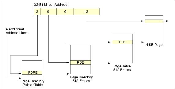
Figure 8-13 PAE-36 address translation
Four reserved bits of control register CR3 pad the existing 32-bit address bus with an additional 4 bits, enabling 36-bit software and hardware addressing to access 64 GB of memory.
PAE maintains the existing Intel 4 KB memory page definition and requires four levels of redirection to generate each physical memory address. However, as memory capacity increases, using a fixed size 4 KB page results in increased memory management overhead, because the number of memory pages grows as the size of maximum addressable memory increases. Using a larger memory page would reduce the total number of pages and the overhead required to point to any one page, because fewer pages would need to be addressed.
PAE is not enabled by default. To use memory beyond 4 GB, you must add the /PAE switch to the corresponding entry in the BOOT.INI file.
PAE is supported only on a 32-bit version of the Windows operating system. 64-bit versions of Windows do not support PAE.
| Note: If you are using a processor with the Data Execution Prevention (DEP) feature (Intel processors
refer to this as Execute Disable Bit or XD feature and AMD processors call this the no-execute page-protection processor
or NX feature) and have it enabled, then Windows Server 2003 32-bit will automatically enable PAE.
To support DEP, Windows will automatically load the PAE kernel no matter how much memory is installed, and you do not have to use the /PAE boot switch in the boot.ini file. |
The following Windows versions support PAE, with the given amount of physical RAM:
|
|
Windows 2000 Advanced Server (8 GB maximum) |
|
|
Windows 2000 Datacenter Server (32 GB maximum) |
|
|
Windows XP (all versions) (4 GB maximum) |
|
|
Windows Server 2003, Standard Edition (4 GB maximum) |
|
|
Windows Server 2003, Enterprise Edition (32 GB maximum) |
|
|
Windows Server 2003, Datacenter Edition (64 GB maximum) |
|
|
Windows Server 2003, Enterprise Edition SP1 (64 GB maximum) |
|
|
Windows Server 2003, Datacenter Edition SP1 (128 GB maximum) |
More importantly for developers and application vendors, the virtual memory limits are increased significantly in all versions of Windows Server 2003, x64 Edition.
| Description | 32-bit | 64-bit (x64) |
|---|---|---|
| Total virtual address space | 4 GB | 16 TB |
| Virtual address space per 32-bit application | 2 GB (Note 1) | 2 GB (Note 2) |
| Virtual address space per 64-bit process | Not applicable | 8 TB |
| Virtual address space for the OS kernel | 2 GB (Note 1) | 8 TB |
| Paged pool | 470 MB | 128 GB |
| Non-paged pool | 256 MB | 128 GB |
| System cache | 1 GB | 1 TB |
| Notes:
1. 3 GB for the application and 1 GB for the kernel if system booted with /3GB switch 2. 4 GB if the 32-bit application has the LARGEADDRESSAWARE flag set (LAA). See "Large |
||
Address Windowing Extensions (AWE) is a set of Windows APIs that implement the PAE functionality of the underlying operating system and allow applications to directly address physical memory above 4 GB.
| Important: The two BOOT.INI switches /PAE and /3GB do interact with each other and in some circumstances should not be used together. See 11.14.1, Interaction of the /3GB and /PAE switches for details. |
The width of a memory address dictates how much memory the processor can address. As shown in Table 8-4, a 32-bit processor can address up to 232 bytes or 4 GB. A 64-bit processor can theoretically address up to 264 bytes or 16 Exabytes (or 16777216 Terabytes).
| Bits (Notation) | Address space |
|---|---|
| 8 (28) | 256 bytes |
| 16 (216) | 65 KB |
| 32 (232) | 4 GB |
| 64 (264) | 18 Exabytes (EB) |
Current implementation limits are related to memory technology and economics. As a result, physical addressing limits for processors are less, as shown in Table 8-5.
Table 8-5
| Processor | Flat addressing | Addressing with PAE |
|---|---|---|
| Intel Xeon MP Gallatin (32-bit) | 4 GB (32-bit) | 128 GB |
| Intel EM64T Nocona (64-bit) | 64 GB (36-bit) | 128 GB in compatibility mode |
| Intel EM64T Potomac (64-bit) | 1 TB (40-bit) | 128 GB in compatibility mode |
| Intel EM64T Cranford (64-bit) | 1 TB (40-bit) | 128 GB in compatibility mode |
| Intel EM64T Paxville (64-bit) | 1 TB (40-bit) | 128 GB in compatibility mode |
| Intel EM64T Tulsa (64-bit) | 1 TB (40-bit) | 128 GB in compatibility mode |
| AMD Opteron (64-bit) | 256 TB (48-bit) | 128 GB in compatibility mode |
Memory supported by processors
These values are the limits imposed by the processors. Memory addressing can be limited further by the chipset or supporting hardware in the server. For example, the System x3950 Potomac-based server addresses up to 512 GB of memory in a 32-way configuration when using 4 GB DIMMs-a technology and physical space limitation.
N-46AMQP
A important component that affects the memory subsystem performance is the BIOS. The first thing to do is to make sure that the last version of the BIOS is installed.
A good example of how a simple BIOS update can improve the memory performance is given by the 1.03 version in the x335. This version introduced a change to enable processor prefetch which increased memory bandwidth (as measured by the Stream Benchmark) by as much as 30%.
Pay close attention to the DIMM configuration of your server. Many servers are designed to provide improved performance when an optimal DIMM configuration is employed. However, the optimal DIMM configuration can be different for each machine.
The rules for memory capacity measurement when upgrading servers that are performing well are straightforward. Usually, the quantity of memory for replacement servers is kept constant or somewhat increased if the number of users and applications does not change. However, this is not always the case.
Most of the memory is used typically for file or data cache for the operating system and applications. The operating system requirement of 128 MB to 256 MB can be ignored for memory capacity analysis because this is usually a small fraction of the required server memory.
The proper approach is to proportionally scale the amount of memory required for the current number of users based on the expected increase of the number of users. For example, a server with 150 users and 2 GB of memory would need 4 GB to support 300 users. Doubling the number of users requires doubling the amount of server memory. To improve the accuracy of memory requirements, the memory usage of the server that is being replaced must be monitored.
There is no guarantee, however, that an existing server always has optimal memory utilization. For Windows environments, you should monitor memory allocation periodically in the Task Manager to determine the amount of total memory that is installed and the average amount of available memory. Total memory minus available memory equals the amount of memory the server is actually using: the working set. Because memory utilization is dynamic, it is best to monitor memory utilization over an extended period of time to arrive at an accurate representation of the memory working set.
A useful rule of thumb to determine the amount of memory that is needed to support twice the number of users is to just double the peak working set size and then add 30% as a buffer for growth activity.
Servers should be configured so that the average memory utilization does not exceed 70% of installed memory. Generally, 30% is enough extra memory so that the server will not expand storage onto disk or page memory onto disk during periods of peak activity. In any event, when you spot excessive memory utilization and the system starts to page, the best fix is to add memory.
The memory rules of thumb are as follows.
http://msdn.microsoft.com/library/default.asp?url=/library/en-us/dng
enlib/html/msdn_manamemo.asp
You should rarely have to worry about providing a separate disk for the page device.
Paging I/O should occur only occasionally, for example when applications are initializing, but generally not on a continuous
basis (unless, of course, you are using an application that employes memory mapped files). In this case, the application
might make heavy use of the paging device, and no increase in memory will reduce the amount of paging activity. For
these applications (typically Lotus Domino and 32-bit SAP R/3), your only option is to move the page file to a high-speed
disk array formatted with a a large stripe size.
Most applications will make use of at least 2 GB of virtual memory. Enterprise
Edition applications will use up to 3 GB of physical memory. If the application is paging and the maximum amount of
memory supported by that application has not been installed, then adding memory is likely to significantly reduce paging.
Unfortunately, some applications will continue to page even after the maximum amount of memory is installed. In this
case, the only choice is to optimize the paging device by using a high-speed disk array.
If time is short, simply determine the amount of installed memory on the server being replaced and scale future memory
requirements based upon the expected increase in the user community. Memory is relatively inexpensive in comparison
to the effort required to accurately predict the exact amount required.
Performance improvements from adding memory can vary greatly because the improvement depends on so many factors, such as the speed of the disk subsystem, the amount of memory the application requires, the speed of your memory subsystem, the speed of the processor, and so forth.
However, Table 8-8 provides a rough idea of the performance improvement you can expect from increasing memory in your server:
Table 8-8
| Memory change | Performance gain |
|---|---|
| 1 to 2 GB | 20% to 50% |
| 2 to 4 GB | 10% to 30% |
| 4 to 8 GB | 15% to 20% |
| 8 to 16 GB | 10% to 20% |
| 16 to 32 GB | 10% to 15% |
| 32 to 64 GB | 5% to 10% |
|
|
Switchboard | ||||
| Latest | |||||
| Past week | |||||
| Past month | |||||
By now, most readers have noticed that the performance of DDR3-1600 reference memory doesn't change. That's because it's always at DDR3-1600 CAS 9, regardless of the data rate its on-paper competition is running. In this case, everything but the reference memory is operating at DDR3-2133, which should kick performance up a couple notches.
Column Address Strobe (CAS) latency, or CL, is the delay time between the moment a memory controller tells the memory module to access a particular memory column on a RAM memory module, and the moment the data from given array location is available on the module's output pins. In general, the lower the CAS latency, the better.
tomshardware.com
2133MHz on any Sandy Bridge is a hit or miss, in by miss I mean BSODs. Yes, you can raise the CAS timings to improve stability e.g. 9-11-9 -> 11-11-11 which is a real JEDEC standard; defeats the Frequency. I find RAM Mfg's try to get the magical CAS 9, but the CAS/frequency of problems warrants a careful look on motivation. IMO - Don't run 2133 MHz on SB, maybe 1866 MHz with a kit that offers a low tight CAS.
I generally recommend 4GB density/stick 1600 MHz CAS 8-8-8, and in the beginning I was an 1866 'pusher' but I was getting some blow-back.
Another nice Article -> http://www.tomshardware.com/review [...] 778-8.html
The 'Wall' 99% of these posts are for gaming, therefore there are a few things to consider:
1. Stability
2. PerformanceMost people aren't multi-tasking freaks they're Gamers and sometimes Render'ers who don't want a BSOD 2 hours into their games or CAD/Rendering work, and the 1600 MHz CAS 8/9 is a WALL to the Games and GB's of RAM to the Render's. There is more than one article to substantiate the benchmarks.
I run 2000MHz on my OC 980X {BCLK + CPU Multiplier} where I can adjust my BCLK to achieve greater stability, those days are gone with Intel, I'd guess for good.
When Intel introduced the Core i7 processor they raised the memory stakes by implementing triple channel memory capability. Instead of two matched pairs of memory sticks, the new x58 motherboards can use matched memory sticks in sets of three. Kingston, known for their acclaimed HyperX memory line have released the Kingston HyperX DDR3 2GHz triple channel memory kit to provide performance memory for the Intel Core i7 platform.One of the performance requirements for the Core i7 machines is that system memory should not run higher than 1.65v to prevent possible damage to the CPU. The kit we will be looking at today is the one of fastest models available and runs at 2GHz / PC3-16000. The Kingston HyperX PC3-16000 kit runs at a 1.5v default and set at 1.65v these sticks easily run at CL9-9-9-27 timings.
Some x58 motherboards feature Intel Extreme Memory Profiles (XMP) which is a high-performance DDR3 memory overclocking tool. Users can take advantage of this memory overclocking tool by making simple adjustments in the BIOS. Even the novice overclockers can take their Core i7 to the next level in no time with Kingston HyperX PC3-16000 kit and an XMP supported motherboard.
If you have purchased Kingston memory in the past, then the Kingston HyperX PC3-16000 kit packaging will be very familiar. The memory sticks are nestled in a clamshell package with the modules sitting in three separate slots and covered by a plastic cover. Sealing the package is a Kingston sticker which lists the model number, memory size, timings and speed.
As befitting a power-user system, the unit I reviewed comes with an Intel Core i7-920 processor and 6GB of DDR3 SDRAM.
You can configure the system with as much as a whopping 24GB of memory (though I don't know how much that would improve performance) and a Core i7-940 or i7-965 Extreme Edition processor.
The Core i7-920 is a solid quad-core processor with HyperThreading, so theoretically it could work on eight streams of data at once, which makes it suitable for multimedia tasks.
My review unit came with a 1GB ATI Radeon HD 4870 graphics card (the top of the line that Dell offers for this model), rendering it capable of playing the latest 3D games, including Crysis and World in Conflict. Note that although the Radeon card itself is CrossFire dual-card capable, the motherboard in the 435 supports only one graphics card.
This server supports ECC and ECC REGISTERED Memory, This server supports 2 CPUs, it takes 12gb maximum memory and 6 sockets (2 banks of 3) per CPU with ECC Memory and it takes 48gb maximum memory and 12 sockets (4 banks of 3) per CPU with ECC REGISTERED Memory. Please refer to the system manual for proper installation of DIMMs for Single, Dual, and Triple Channel configurations.
Google matched content |
Society
Groupthink : Two Party System as Polyarchy : Corruption of Regulators : Bureaucracies : Understanding Micromanagers and Control Freaks : Toxic Managers : Harvard Mafia : Diplomatic Communication : Surviving a Bad Performance Review : Insufficient Retirement Funds as Immanent Problem of Neoliberal Regime : PseudoScience : Who Rules America : Neoliberalism : The Iron Law of Oligarchy : Libertarian Philosophy
Quotes
War and Peace : Skeptical Finance : John Kenneth Galbraith :Talleyrand : Oscar Wilde : Otto Von Bismarck : Keynes : George Carlin : Skeptics : Propaganda : SE quotes : Language Design and Programming Quotes : Random IT-related quotes : Somerset Maugham : Marcus Aurelius : Kurt Vonnegut : Eric Hoffer : Winston Churchill : Napoleon Bonaparte : Ambrose Bierce : Bernard Shaw : Mark Twain Quotes
Bulletin:
Vol 25, No.12 (December, 2013) Rational Fools vs. Efficient Crooks The efficient markets hypothesis : Political Skeptic Bulletin, 2013 : Unemployment Bulletin, 2010 : Vol 23, No.10 (October, 2011) An observation about corporate security departments : Slightly Skeptical Euromaydan Chronicles, June 2014 : Greenspan legacy bulletin, 2008 : Vol 25, No.10 (October, 2013) Cryptolocker Trojan (Win32/Crilock.A) : Vol 25, No.08 (August, 2013) Cloud providers as intelligence collection hubs : Financial Humor Bulletin, 2010 : Inequality Bulletin, 2009 : Financial Humor Bulletin, 2008 : Copyleft Problems Bulletin, 2004 : Financial Humor Bulletin, 2011 : Energy Bulletin, 2010 : Malware Protection Bulletin, 2010 : Vol 26, No.1 (January, 2013) Object-Oriented Cult : Political Skeptic Bulletin, 2011 : Vol 23, No.11 (November, 2011) Softpanorama classification of sysadmin horror stories : Vol 25, No.05 (May, 2013) Corporate bullshit as a communication method : Vol 25, No.06 (June, 2013) A Note on the Relationship of Brooks Law and Conway Law
History:
Fifty glorious years (1950-2000): the triumph of the US computer engineering : Donald Knuth : TAoCP and its Influence of Computer Science : Richard Stallman : Linus Torvalds : Larry Wall : John K. Ousterhout : CTSS : Multix OS Unix History : Unix shell history : VI editor : History of pipes concept : Solaris : MS DOS : Programming Languages History : PL/1 : Simula 67 : C : History of GCC development : Scripting Languages : Perl history : OS History : Mail : DNS : SSH : CPU Instruction Sets : SPARC systems 1987-2006 : Norton Commander : Norton Utilities : Norton Ghost : Frontpage history : Malware Defense History : GNU Screen : OSS early history
Classic books:
The Peter Principle : Parkinson Law : 1984 : The Mythical Man-Month : How to Solve It by George Polya : The Art of Computer Programming : The Elements of Programming Style : The Unix Hater’s Handbook : The Jargon file : The True Believer : Programming Pearls : The Good Soldier Svejk : The Power Elite
Most popular humor pages:
Manifest of the Softpanorama IT Slacker Society : Ten Commandments of the IT Slackers Society : Computer Humor Collection : BSD Logo Story : The Cuckoo's Egg : IT Slang : C++ Humor : ARE YOU A BBS ADDICT? : The Perl Purity Test : Object oriented programmers of all nations : Financial Humor : Financial Humor Bulletin, 2008 : Financial Humor Bulletin, 2010 : The Most Comprehensive Collection of Editor-related Humor : Programming Language Humor : Goldman Sachs related humor : Greenspan humor : C Humor : Scripting Humor : Real Programmers Humor : Web Humor : GPL-related Humor : OFM Humor : Politically Incorrect Humor : IDS Humor : "Linux Sucks" Humor : Russian Musical Humor : Best Russian Programmer Humor : Microsoft plans to buy Catholic Church : Richard Stallman Related Humor : Admin Humor : Perl-related Humor : Linus Torvalds Related humor : PseudoScience Related Humor : Networking Humor : Shell Humor : Financial Humor Bulletin, 2011 : Financial Humor Bulletin, 2012 : Financial Humor Bulletin, 2013 : Java Humor : Software Engineering Humor : Sun Solaris Related Humor : Education Humor : IBM Humor : Assembler-related Humor : VIM Humor : Computer Viruses Humor : Bright tomorrow is rescheduled to a day after tomorrow : Classic Computer Humor
The Last but not Least Technology is dominated by two types of people: those who understand what they do not manage and those who manage what they do not understand ~Archibald Putt. Ph.D
Copyright © 1996-2021 by Softpanorama Society. www.softpanorama.org was initially created as a service to the (now defunct) UN Sustainable Development Networking Programme (SDNP) without any remuneration. This document is an industrial compilation designed and created exclusively for educational use and is distributed under the Softpanorama Content License. Original materials copyright belong to respective owners. Quotes are made for educational purposes only in compliance with the fair use doctrine.
FAIR USE NOTICE This site contains copyrighted material the use of which has not always been specifically authorized by the copyright owner. We are making such material available to advance understanding of computer science, IT technology, economic, scientific, and social issues. We believe this constitutes a 'fair use' of any such copyrighted material as provided by section 107 of the US Copyright Law according to which such material can be distributed without profit exclusively for research and educational purposes.
This is a Spartan WHYFF (We Help You For Free) site written by people for whom English is not a native language. Grammar and spelling errors should be expected. The site contain some broken links as it develops like a living tree...
|
|
You can use PayPal to to buy a cup of coffee for authors of this site |
Disclaimer:
The statements, views and opinions presented on this web page are those of the author (or referenced source) and are not endorsed by, nor do they necessarily reflect, the opinions of the Softpanorama society. We do not warrant the correctness of the information provided or its fitness for any purpose. The site uses AdSense so you need to be aware of Google privacy policy. You you do not want to be tracked by Google please disable Javascript for this site. This site is perfectly usable without Javascript.
Last modified: March, 12, 2019